Product Performance
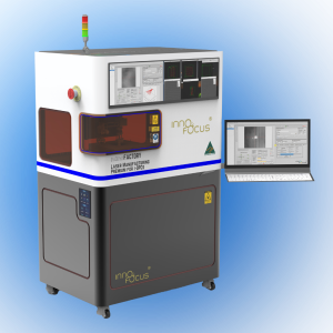
Innofocus developed the world-leading intelligent laser nanoprinting system, capable of fabricating arbitrarily designed 3D nano-structures with ultra-high precision (1000 times higher than commercial 3D-print), high yield and stability. It solves the low productivity bottleneck and simultaneously improves the quality, energy-efficiency of the fabrication process, promoting cost-effectiveness and competitiveness of Australian advanced manufacturing industry.
This fully Australian-developed technology with complete IP ownership addresses critical gaps in the international market through three revolutionary advances:
Unmatched precision at industrial scale
Surpassing Germany’s market-leading systems, deliver <10 nm accuracy at 400x the speed of conventional methods – a feat previously unattainable outside elite facilities. Unlike competitors requiring million-dollar cleanrooms, our AI-driven automation enables atomic-scale fabrication in standard-lab conditions, democratising access to quantum-grade manufacturing.
Quantum photonics enabler
As the only commercially available system capable of mass-producing quantum photonic chips, our technology solves the critical bottleneck in photonic quantum computing:
- 3D nanostructuring of waveguides and beam splitters with 50 nm fidelity
- Monolithic integration of quantum light sources and detectors
- Scalable yield (98% first-pass success) unachievable with electron-beam lithography
Strategic manufacturing sovereignty
With export to overseas, we’ve proven our capacity to outperform international competitors. It represents Australia’s best opportunity to lead $280 Bn quantum photonics market (McKinsey):
- Establish sovereign capability in quantum device production.
- Capture >15% of global nanomanufacturing equipment market.
- Enable Australian researchers to commercialise quantum breakthroughs without offshore fabrication.
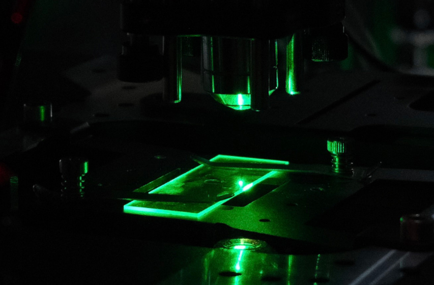
Fabricate arbitrary 3D nanostructures
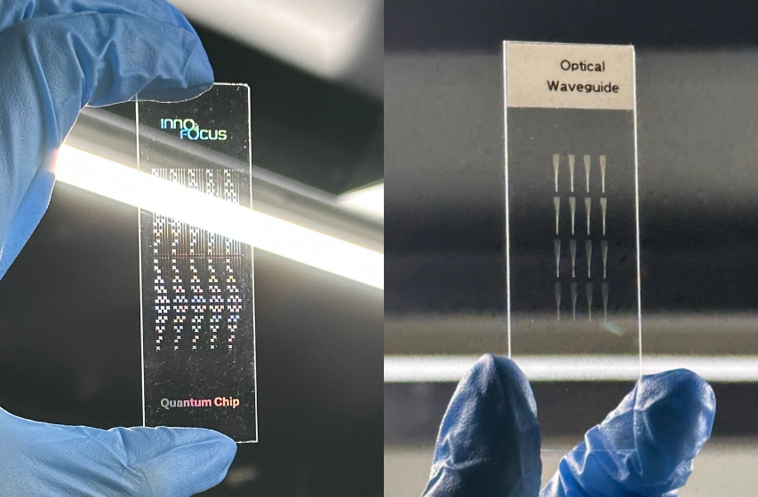
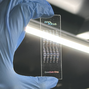
QPC design and prototype
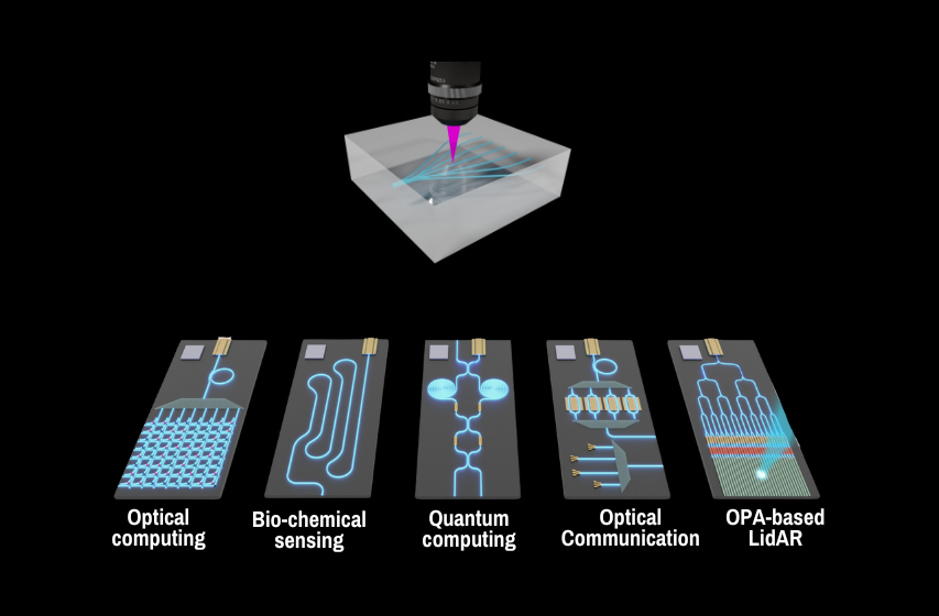
More QPC applications and prototypes
Applications

Optical communications

Quantum tehcnology