
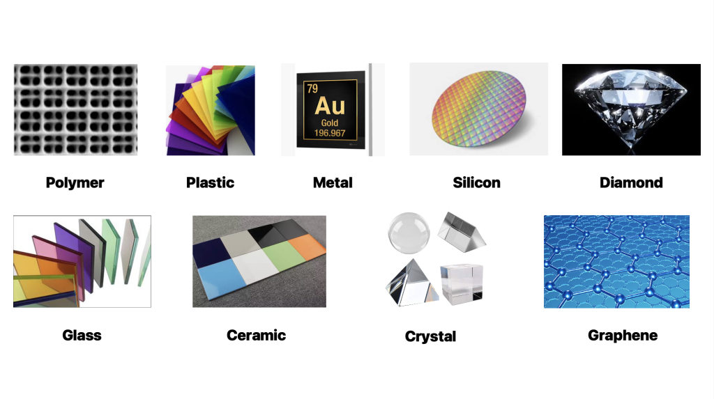
Multi-Material Applicable Laser Processing
Based on these market needs, Innofocus introduces high-power femtosecond lasers with tuneable repetition rate (1kHz-500 kHz) and high-pulse energy (up…
More
Position-Time Synchronised Trigger (PTST)
Innofocus have developed the PTST (Position-Time Synchronised Trigger) module. The PTST technology has been integrated into Innofocus’ world-leading nanoLAB 3D…
More
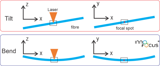
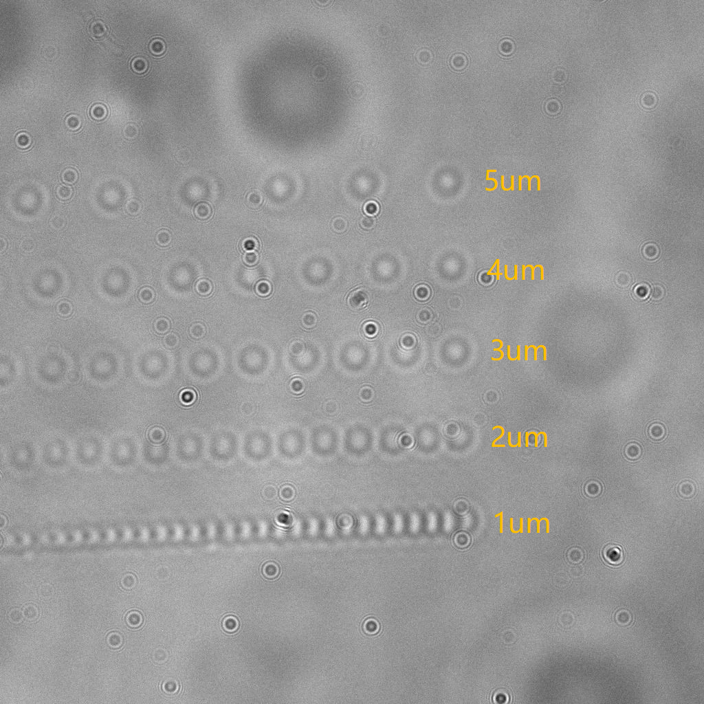
Automatic Fibre Core Tracing Technology
Innofocus also developed automatic fibre core tracing function enabled by AI-vision. It can automatically identify the fiber core and monitor…
More
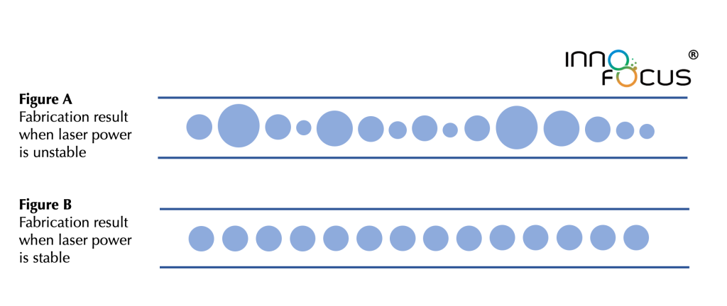
PowerFlex Control Module
High power stability and precise power control are essential to guarantee the high-quality manufacturing of fibre Bragg grating (FBG). PowerFlex…
More
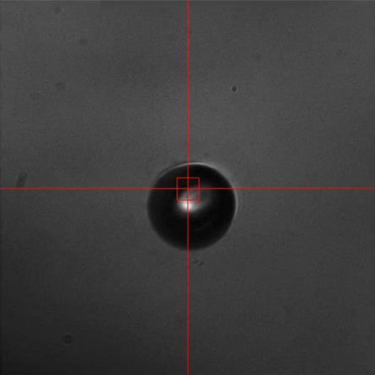
Surface Autotracing Technology
AI-Vision assisted surface autotracing technology developed by Innofocus allows the nanofabrication system to automatically trace the surface of the material…
More
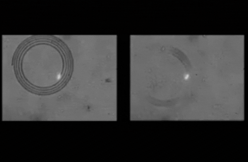
Surface Autolanding Technology
AI-Vision assisted surface autolanding technology developed by Innofocus includes a 3-step process as shown in these images
More

Optical Waveguide
Optical waveguide is a structure that can confine and guide light waves, which is one…
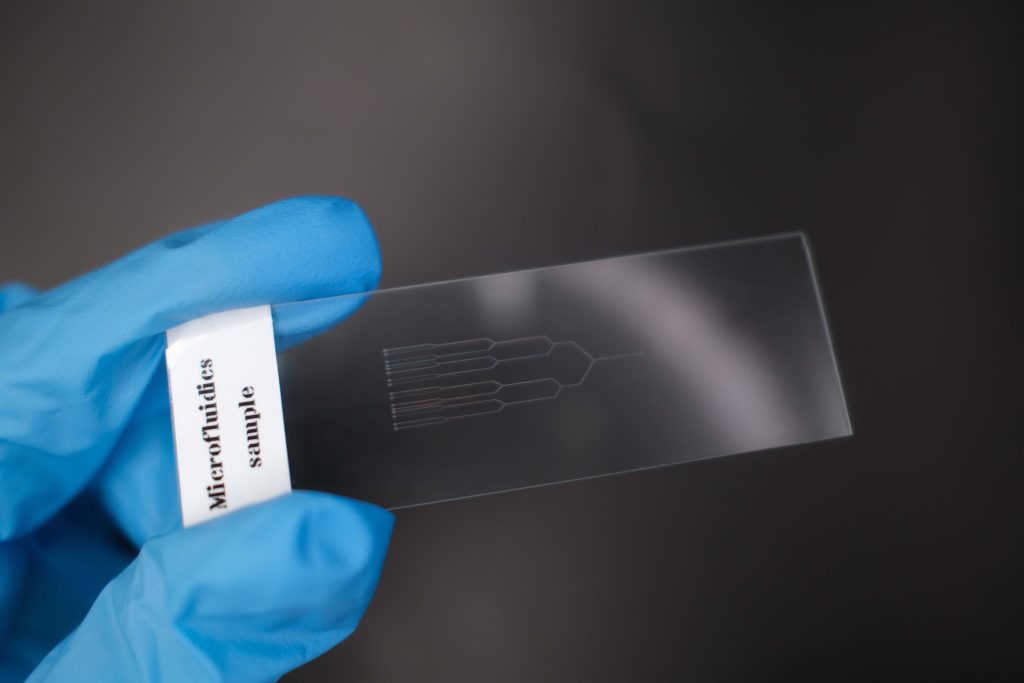
Microfluidic
Microfluidic devices have become a platform for high-throughput sorting, analysis, and assembly in the pharmaceutical…

Quantum Photonic Chips Prototyping
We Are Building Capabilities for QPC design, simulation, manufacturing and characterisation
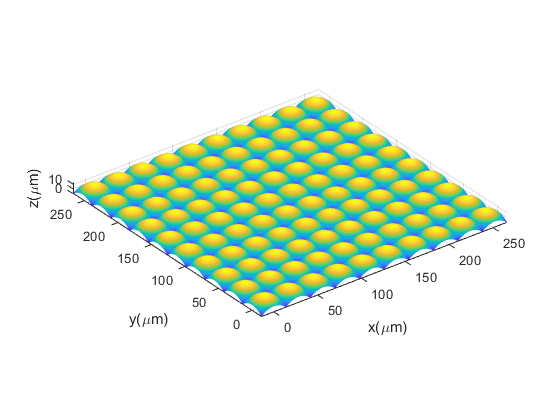
Microlens Array
A micro lens array is an optical component with a surface made of many tiny,…

Highly Encrypted Nanoprinted Colorful Digital ID Tags
Nano Colour Digital ID improves data security.
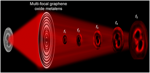
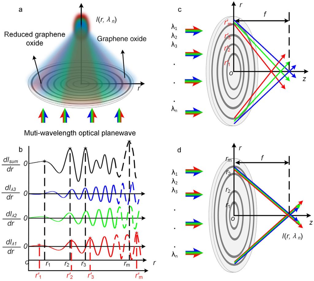
Two Hundred Nanometer Thin Multifocal Graphene Oxide Metalens for Varying Magnification Broadband Imaging
Conventional microscopes, which rely on multiple objective lenses for varying magnifications, are bulky, complex, and costly, making them difficult to…
Multi-Wavelength Achromatic Graphene Metalenses for Visible, NIR, and Beyond
The demand for achromatic ultrathin flat lenses has become increasingly stringent, particularly for high-performance imaging and display applications. Despite significant…
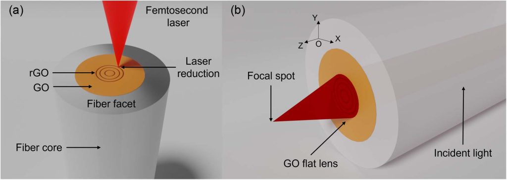
Ultra-high NA graphene oxide flat lens on a fiber facet with near diffraction-limited focusing
The realization of a high numerical aperture (NA) fiber lens is critical for achieving high imaging resolution in endoscopes, enabling…
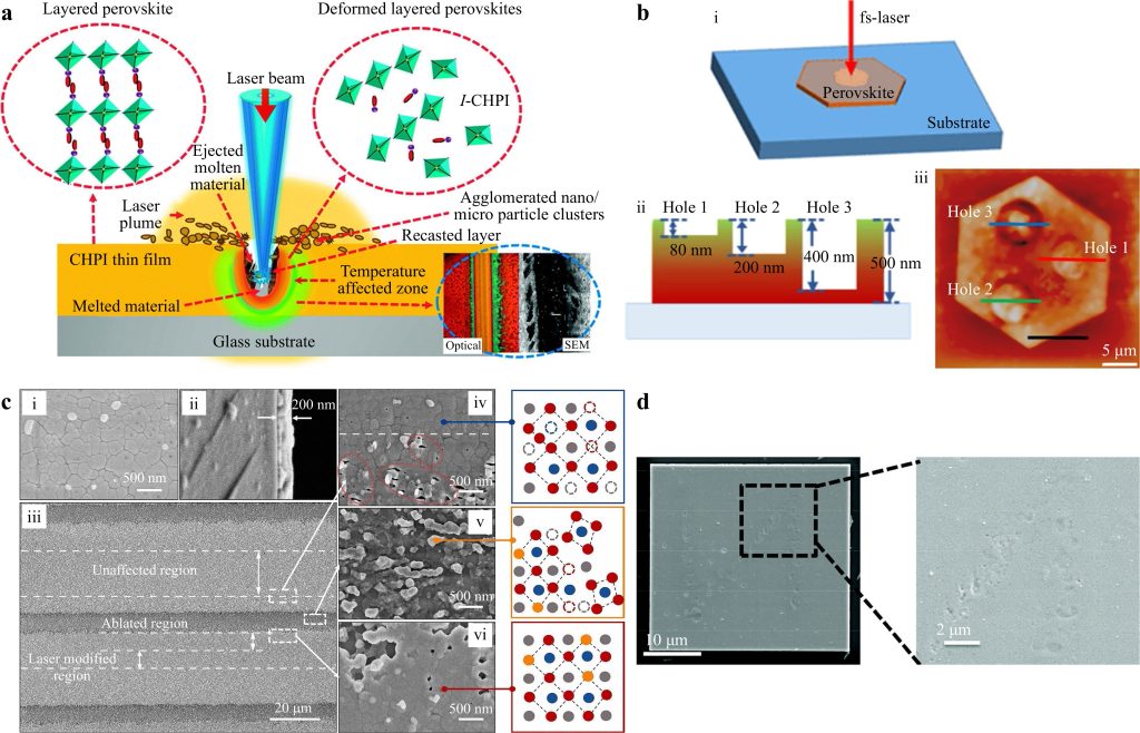
Direct laser writing on halide perovskites: from mechanisms to applications
Metal halide perovskites have emerged as game-changing semiconductor materials in optoelectronics. As an efficient micro-/nano-manufacturing technology, direct laser writing (DLW)…
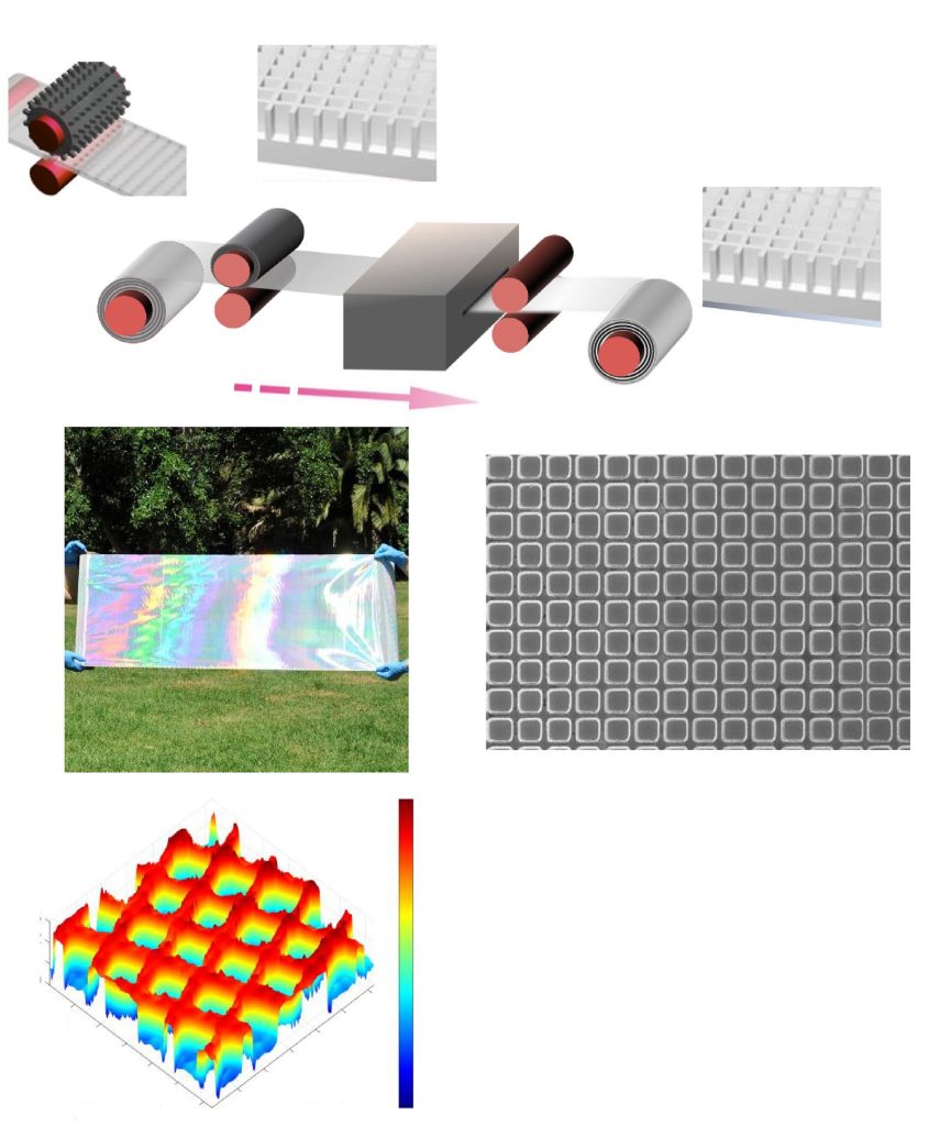
Highly efficient flexible structured metasurface by roll‑to‑roll printing for diurnal radiative cooling
An ideal radiative cooler requires accurate spectral control capability to achieve efficient thermal emission in the atmospheric transparency window (8–13…
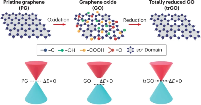
Graphene oxide for photonics, electronics and optoelectronics
Graphene oxide (GO) was initially developed to emulate graphene, but it was soon recognized as a functional material in its…