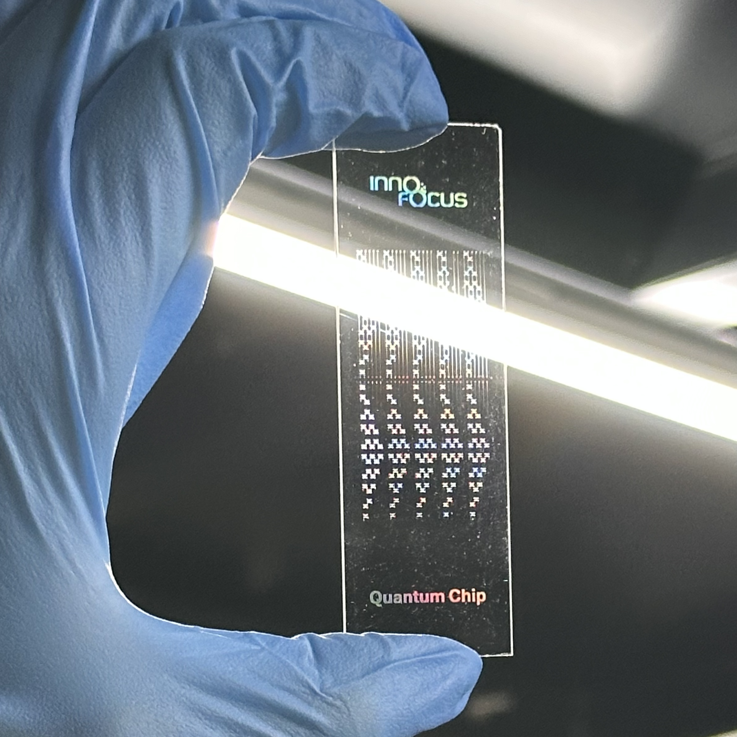
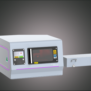
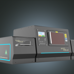
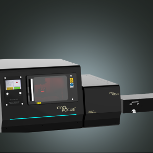
Innofocus NanoPrint 3D Intelligent Laser Nanofabrication System meets the customers’ needs from both academia and industry.
For scientific research
The rapid advancement of information technologies in the 21st century has indicated the approaching post-Moore’s law era. Moore’s law, which dictates the doubling of transistors on microchips every two years, has driven traditional computing technology for many years. The demand for higher speed, larger bandwidth, lower energy consumption, and improved security and stability in information technologies continues to grow. However, as we near the physical limits of miniaturization, new approaches are needed to continue advancing computation.
Integrated Quantum Photonic Chips (i-QPC) have emerged as a promising successor to silicon chips. With the continuous development, i-QPCs which offer the desired features including high speed and low power consumption, has become the best solution for high-throughput communication technology. However, as i-QPCs move towards commercialization and industrialization, existing fabrication capabilities face significant challenges concerning precision, reproducibility, and scalability to fulfil the needs for R&D and manufacturing.
Conventional configuration of a laser nanofabrication system involves the segregation of distinct modules, with one dedicated to the fabrication process and another intended for characterisation purposes. Therefore, users have to remove the fabricated sample in order to characterize it and then optimize the outcome, leading to a multi-stage and time-consuming process. This hence presents a challenge to the quality control of photonic chips and i-QPC. Additionally, the multi-stage process can introduce error, which results in insufficient correlations between the characterization results and the fabrication parameters.
To efficiently and accurately characterize nanostructure/nanopatterns of 3D photonic chips has been long sought. However, we are yet to find a method that can accurately characterize the refractive index distribution as well as the surface morphology of the optical materials. To fabricate 3D optical structures in optical crystals, the difference in refractive index introduced by laser processing is particularly important, which determines the design of the optical component and its loss.
To efficiently and accurately characterise nanostructure/nanopatterns of 3D photonic chips has been long sought. However we are yet to find a method that can accurately characterize the refractive index distribution as well as the surface morphology of the optical materials. To fabricate 3D optical structures in optical crystals, the difference in refractive index introduced by laser processing is particularly important, which determines the design of the optical component and its loss.
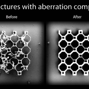
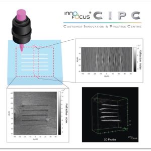
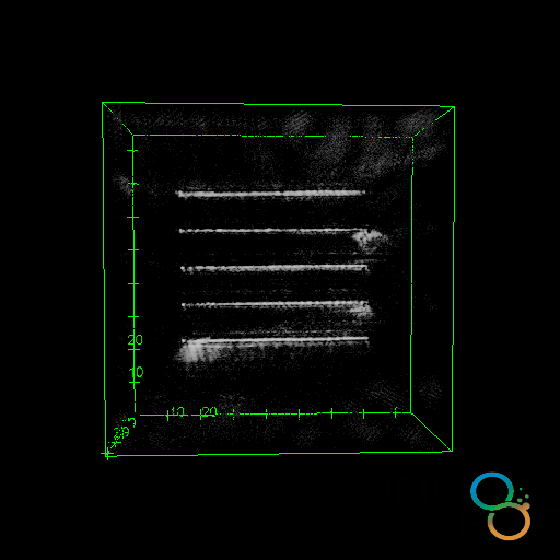
HoloView 3DRI, the 3D in-situ refractive index characterisation system designed by Innofocus, has proved to enable characterize the 3D spatial refractive index distribution with our innovative optical imaging technology and image reconstruction algorithm. The system can precisely measure the refractive index distribution in material and effectively reconstruct the refractive index distribution, and form image of the 3D structure with an accuracy of 10-4. It is non-destructive and non-invasive, and it allows on-line inspection of the fabrication outcomes and on-site correction of fabrication conditions, making it valuable for the applications in the disciplines of 3D photonic chips, all-optical communications, sensors, biophotonic and micro/nano optical and photonic devices.
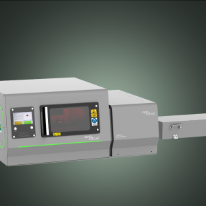
The key functions of the HoloView 3DRI system developed by Innofocus include:
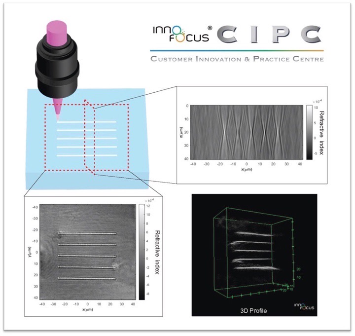
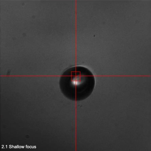
Innofocus Photonics Technology Pty Ltd
Unit 10/17 Helen Street, Heidelberg West 3081, Victoria, Australia
Fill out the form below and we'll get back to you as soon as possible.
"*" indicates required fields